
 Relative importance of the three different initial valley arrangements for electrons in the eeh process, which are illustrated in (b) with the f-type arrangement contributing most strongly. Strength of phonon-assisted AMR for eeh (solid black) and hhe (red dash) processes as a function of phonon energy (c) and wave vector magnitude (d), where the strongest peaks are associated with TA phonons, highlighted in the inset phonon dispersion. (e) The distribution of excited carrier states throughout the first Brillioun zone for the direct and phonon-assisted eeh and phonon-assisted hhe processes, with slices removed to show the internal structure. Credit: Kyle Bushick, University of Michigan")
Silicon is one of the most pervasive functional materials of the modern age, underpinning semiconductor technologies ranging from microelectronics to solar cells. Indeed, silicon transistors enable computing applications from cell phones to supercomputers, while silicon photovoltaics are the most widely deployed solar-cell technology to date.
The U.S. Department of Energy (DOE) reports that nearly 50% of new electric generation capacity in 2022 came from solar cells, and according to the International Energy Agency (IEA), silicon has a 95% market share. Yet despite silicon’s undisputed importance to our modern way of life, many open questions remain about its fundamental physical properties.
In semiconductor devices, the functionality of the material comes from the motion and interactions of subatomic particles such as electrons (which have negative charge) and holes (the absence of an electron from an otherwise occupied state that itself behaves like a positively charged particle), which are called carriers as they “carry” electrical charge through the material.
For example, in a solar cell, the material absorbs incoming light, and the absorbed energy is converted into pairs of electrons and holes. These excited electron and holes then move to opposite ends of the solar cell and generate electricity.
Unfortunately, the electrons and holes can also interact in undesirable ways that convert their energy to heat and limit the efficiency of devices. One such loss mechanism occurs when carriers recombine and convert their energy to heat by interacting with a defect in the material. In many cases this defect-mediated recombination can be reduced by improving the quality of the material.
Other interactions, however, are intrinsic to a material and cannot be eliminated even in perfectly pure samples. Auger-Meitner recombination (AMR), historically known also as Auger recombination, is one such interaction. It is named after Lise Meitner and Pierre Auger, two pioneers of nuclear science who independently discovered this effect in atoms.
The new naming convention of the Auger-Meitner effect recognizes the contributions of Lise Meitner, a female Austrian physicist and the eponym of the Meitnerium chemical element, who independently discovered the process a year prior to Pierre Auger.
In the AMR process in semiconductors, one electron and one hole recombine, transferring their energy to a third carrier. The high-energy carrier can then thermalize or leak out of a device, generating heat and reducing the energy-conversion efficiency or reducing the number of available carriers. Unfortunately, despite decades of research, the specific atomistic mechanisms of AMR in silicon have eluded researchers to this date.
With a new implementation of a computational methodology to accurately calculate AMR rates from first principles—that is using only the physical constants of the universe and the atomic number of silicon as input—Dr. Kyle Bushick and Prof. Emmanouil Kioupakis of Materials Science and Engineering at the University of Michigan have provided the first comprehensive characterization of this important recombination process in silicon. This computational approach is key to gaining a full understanding of the AMR mechanism, because it is a process that does not emit light, making it very difficult to study in the lab.
With the aid of supercomputing resources at the National Energy Research Scientific Computing Center (NERSC) of Lawrence Berkeley National Lab, Bushick and Kioupakis were able to carry out the calculations of AMR in silicon, gaining insights to the behavior of the material at an atomic level.
One reason the AMR process in silicon has not been fully understood is that it includes multiple permutations. On one hand, the excited (third) carrier can either be an electron, or a hole, giving rise to the electron-electron-hole (eeh) and hole-hole-electron (hhe) processes, respectively.
Furthermore, AMR can be both direct, where only the three carriers participate, or phonon-assisted, where one of the carriers interacts with the vibrating atoms (phonons) to transfer additional momentum. While experiments can characterize the combined total AMR rate, parsing out the different contributions from these different components can be much harder. However, by using predictive atomistic calculations, each individual component can be directly computed and characterized.
Although past work had investigated the direct process using such calculations, it was clear that the direct process alone didn’t capture the full experimental picture. By overcoming the added complexity of calculating both the direct and phonon-assisted processes at the same level of theory, many of the unanswered questions about AMR in silicon could be addressed. Additionally, achieving such a detailed understanding of the process then opens the door for finding solutions to reduce the impact of AMR on device efficiency.
In their report, published in Physical Review Letters, Bushick and Kioupakis unequivocally elucidate the importance of the phonon-assisted AMR process in silicon.
“We found that the electron-phonon interactions not only account for the entirety of the hhe process, which was hypothesized in previous works but never conclusively demonstrated, but also for a significant portion of the eeh process, a finding that had been a subject of unresolved debate in the literature,” says Bushick, a recently graduated Ph.D. student of Materials Science and Engineering and a DOE Computational Science Graduate Fellow.
Furthermore, they highlight a potential pathway for altering AMR in silicon by applying strain to the material, a conclusion made possible by their newly implemented methodology.
This work provides a hitherto inaccessible fundamental understanding of an important intrinsic loss mechanism in the world’s most important semiconductor. This understanding, which has eluded scientists for decades, can help design better devices with improved performance by reducing the occurrence of the undesirable AMR process.
Emmanouil Kioupakis, Associate Professor of Materials Science and Engineering and Karl F. and Patricia J. Betz Family Faculty Scholar at the University of Michigan notes, “Ultimately, this work paves the way to understand and mitigate losses in silicon devices such as transistors or solar cells. Considering the size of these industries, even small improvements can lead to massive benefits.”
More information: Kyle Bushick et al, Phonon-Assisted Auger-Meitner Recombination in Silicon from First Principles, Physical Review Letters (2023). DOI: 10.1103/PhysRevLett.131.076902
Journal information: Physical Review Letters
Provided by University of Michigan


 and the magic-angle graphene moiré superlattice (right panel). Credit: Kevin Nuckolls, Yazdani Group, Princeton University")


. DOI: 10.1016/j.talanta.2023.125067")


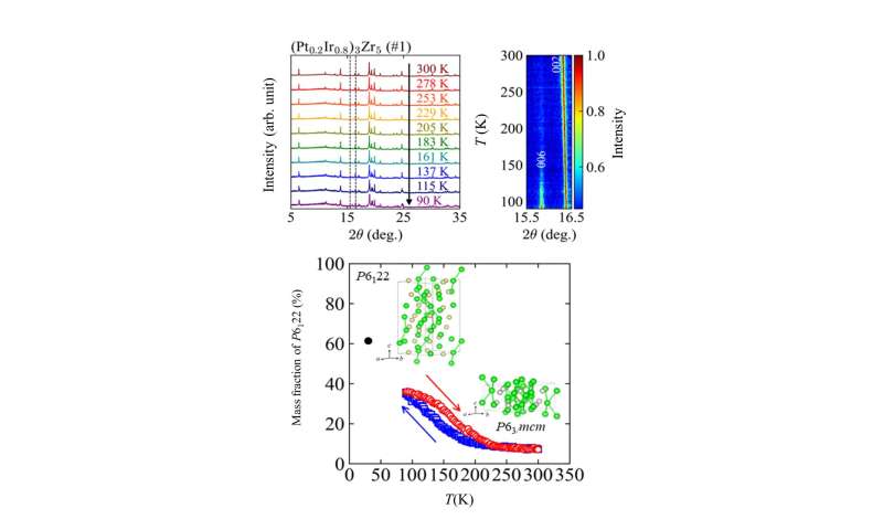 X-ray diffraction patterns at different temperatures (top), and the extracted fraction of chiral compound (bottom) show that the proportion of chiral compound increases at lower temperature. Credit: Tokyo Metropolitan University
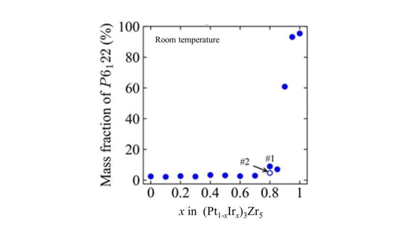 As the proportion of iridium is increased, the proportion of P6122, the chiral component, increases. Credit: Tokyo Metropolitan University
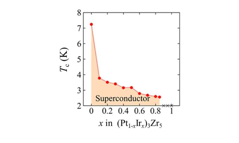 Superconductivity can be confirmed below an iridium proportion of around x = 0.85 in (Pt1-xIrx)3Zr5. Credit: Tokyo Metropolitan University
 from all other nuclei created in a complex nuclear reaction (left) and the resulting ability to gain knowledge of the unique sulfur-38 quantum \"fingerprint\" (right). Credit: Argonne National Laboratory")

 and optical microscopy image (b) of the MEMS-based 2 × 2 unitary gate. The gate consists of one phase shifter and one tunable coupler. The equation in a shows the mathematical description of the ideal 2 × 2 unitary transformation gate without any optical losses. Credit: Nature Photonics (2023). DOI: 10.1038/s41566-023-01327-5")

